.D5CzYVR1.png)


Domestic low-light CMOS imaging component series
Product usage
Application scenarios
GS12542A Micro Light CMOS Imaging Component
Description:
The GS12553A low-light CMOS imaging module utilizes a low-noise, low-illuminance, rolling shutter high-definition CMOS image sensor to create a domestically produced high-definition monochrome low-light digital camera. This module features automatic exposure, defect compensation, 3D noise reduction, HDR, image enhancement, high near-infrared response sensitivity, windowed output, and fog penetration capabilities. Its minimum illumination can reach 6.5 × 10⁻⁴ Lux, and back-illuminated CIS can reach 5 × 10⁻⁴ Lux.
Specifications:
⚫ Near-infrared enhanced,
⚫ low noise,
⚫ full HD,
⚫ low-light night vision,
⚫ fog penetration.
Applications:
⚫ Vehicle-mounted observation and monitoring
⚫ Machine vision
⚫ Security monitoring
⚫ Tracking and recognition
Characteristics:
Sensor:9.7um×9.7um,1 inch CMOS
Resolution:1280(H) x 1024(V)
FWC: 6 ke- (high gain) 50 ke- (low gain)
Readout Noise:1.5 e- (high gain)
Frame rate:30Hz/60Hz
FPN:1.5lsb
PRNU:≤2%
Dynamic Range:≥80dB(HDR) ≥68dB(non HDR)
Defect Pixel Correction:Yes
Electronic Shutter:Rolling Shutter
Gain:0-24dB
Video Output:CameraLink
Monochrome / Color:Monochrome
Output Clock Speed:50MHz
MIN Illumination:6.5×10⁻⁴ Lux、5×10⁻⁴ Lux(Back-illuminated CIS, field test in Wuhai, focal length 35mm@F1.4)
Power Input:4 - 6V
Power Dissipation :≤2W
Operating Temperature:-55℃ - +70℃
Sensor Position:Structural geometric center
Reliability:Random vibration, impact
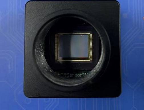
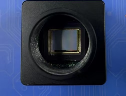
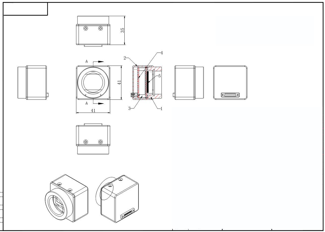
Dimensional outlines:
The package:
“:
Definition of pins:
Interface distribution:
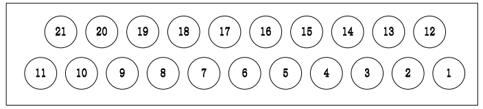
Definition of pins:
Interface Signal Description Signal Name
21 Cameralink Clock Negative CL_CLK-
20 Cameralink Clock Positive CL_CLK+
19 Cameralink TX3 Negative CL_TX3-
18 Cameralink TX3 Positive CL_TX3+
17 Cameralink TX2 Negative CL_TX2-
16 Cameralink TX2 Positive CL_TX2+
15 Cameralink TX1 Negative CL_TX1-
14 Cameralink TX1 Positive CL_TX1+
13 Cameralink TX0 Negative CL_TX0-
12 Cameralink TX0 Positive CL_TX0+
11 RS422 Transmit Signal Negative DI-
10 RS422 Transmit Signal Positive DI+
9 RS422 Receive Signal Negative RO-
8 RS422 Receive Signal Positive RO+
7 Signal Ground GND
6 Reserved Signal Reserved
5 Reserved Signal Reserved
4 Reserved Signal Reserved
3 Reserved Signal Reserved
2 Ground GND
1 Power Input +5V VCC_IN
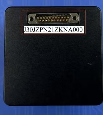
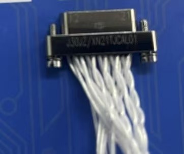
Note: The connector used on the component is the J30JZPN21ZKNA000 female connector from Shaanxi Huada Company, as shown in the figure.
The mating male connector is J30JZ/XN21TJCAL01, as shown in the figure below.
GS12553A Micro Light CMOS Imaging Component
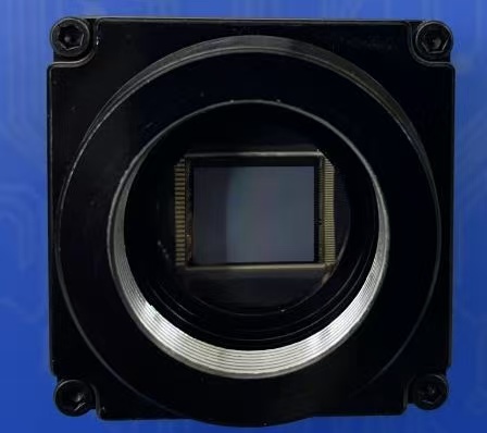
Description:
The GS12553A low-light CMOS imaging module is designed as a domestically produced high-definition monochrome low-light digital camera using a low-noise, low-illuminance, rolling shutter high-definition CMOS image sensor. This module features automatic exposure, defect compensation, 3D noise reduction, HDR, image enhancement, high near-infrared response sensitivity, windowed output, and fog penetration. Its minimum illumination can reach 6.5×10⁻⁴ Lux, and back-illuminated CIS can reach 5×10⁻⁴ Lux.
Specifications:
⚫ Near-infrared enhanced,
⚫ low noise,
⚫ full HD,
⚫ low-light night vision,
⚫ fog penetration.
Applications:
⚫ Vehicle-mounted observation and monitoring
⚫ Machine vision
⚫ Security monitoring
⚫ Tracking and recognition
Characteristics:
Sensor :9.7um×9.7um,1 英寸 CMOS
Resolution :1280(H) x 1024(V)
FWC :6 ke- (high gain),50 ke- (low gain)
Readout Noise :1.5 e- (high gain)
Frame rate::30Hz
FPN :1.5lsb
PRNU: ≤2%
Dynamic Range: ≥80dB(HDR) ≥68dB(non HDR)
Defect Pixel Correction :Yes
Electronic Shutter :Rolling Shutter
Gain: 0-24dB
Video Output :Gigabit Ethernet (UDP protocol)
Monochrome / Color :Monochrome
Output Clock Speed 125MHz
MIN Illumination :6.5×10⁻⁴ Lux、
5×10⁻⁴ Lux(Back-illuminated CIS, field test in Wuhai, focal length 35mm@F1.4)
Power Input :4 - 6V
Power Dissipation :≤2W
Operating Temperature: -55℃ - +70℃
Sensor Position :Structural geometric center
Reliability :Random vibration, impact
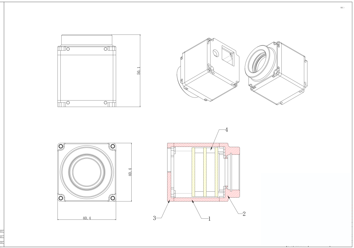
Dimensional outlines:
The package:
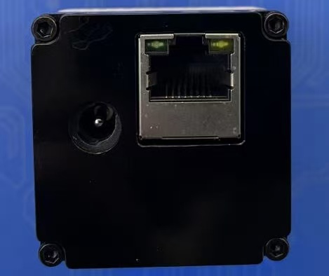
Definition of pins:
Interface distribution:
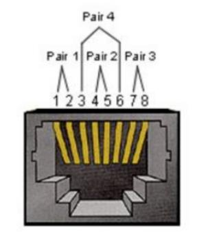
Definition of pins:
Pin Number Pin Name Function Description
PIN1 TX_D1+ Transmit Data +
PIN2 TX_D1- Transmit Data -
PIN3 RX_D2+ Receive Data +
PIN4 BI_D3+ Bidirectional Data +
PIN5 BI_D3- Bidirectional Data -
PIN6 RX_D2- Receive Data-
PIN7 BI_D4+ Bidirectional Data +
PIN8 BI_D4- Bidirectional Data -
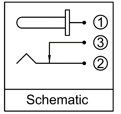
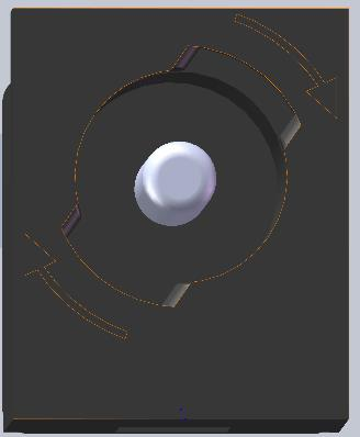
Note: The power connector used on this component is a standard PowerJACK. The schematic and outline are shown in the figures. The center pin diameter is 2mm. The component input voltage is 5V, and the maximum current is 0.4A. Hot-plugging is not supported!
GS12554A Micro Light CMOS Imaging Component
Description:
The GS12554A low-light CMOS imaging module utilizes a low-noise, low-illuminance, rolling shutter high-definition CMOS image sensor to create a domestically produced high-definition monochrome low-light digital camera. This module features automatic exposure, defect compensation, 3D noise reduction, HDR, image enhancement, high near-infrared response sensitivity, windowed output, and fog penetration capabilities. Its minimum illumination can reach 6.5×10⁻⁴ Lux, and back-illuminated CIS can reach 5×10⁻⁴ Lux.
Specifications:
⚫ Near-infrared enhanced,
⚫ low noise,
⚫ full HD,
⚫ low-light night vision,
⚫ fog penetration.
Applications:
⚫ Gun sights
⚫ Individual helmet
⚫ Binoculars
Characteristics:
Sensor: 9.7um×9.7um,1 英寸 CMOS
Resolution: 1280(H) x 1024(V)
FWC :6 ke- (high gain),50 ke- (low gain)
Readout Noise :1.5 e- (high gain)
Frame rate :30Hz/60Hz
FPN: 1.5lsb
PRNU: ≤2%
Dynamic Range :≥80dB(HDR) ≥68dB(non HDR)
Defect Pixel Correction :Yes
Electronic Shutter :Rolling Shutter
Gain: 0-24dB
Video Output: CameraLink/OLED
Monochrome / Color: Monochrome
Output Clock Speed: 50MHz
MIN Illumination :6.5×10⁻⁴ Lux、5×10⁻⁴ Lux(Back-illuminated CIS, field test in Wuhai, focal length 35mm@F1.4)
Power Input: 4 - 6V
Power Dissipation :≤1.5W
Operating Temperature :-40℃ - +60℃
Sensor Position: Structural geometric center
Reliability: Random vibration, impact
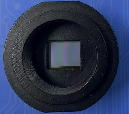
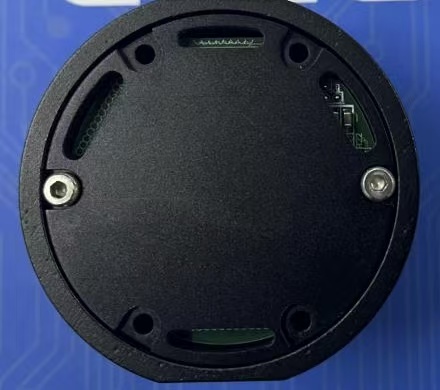
Dimensional outlines:
The package:
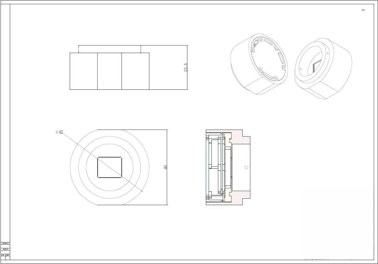
Definition of pins:
Interface distribution:
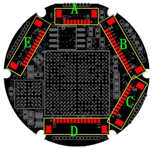
Definition of pins:
Pin Number | Pin Name | Function Description
A01 | FPGA_TCK | Debug Clock Signal Output
A02 | GND | Ground
A03 | FPGA_TDO | Debug Data Output
A04 | +3.3VD | 3.3V Power Supply
A5 | FPGA_TMS | Debug Mode Selection Signal Input
A06 | NC | Unused
A07 | FPGA_TDI | Debug Data Input
A08 | GND | Ground
B01 | P_DATA8 | Display Data Signal
B02 | P_DATA9 | Display Data Signal
B03 | P_DATA10 | Display Data Signal
B04 | P_DATA11 | Display Data Signal
B05 | P_DATA12 | Display Data Signal
B06 | P_DATA13 | Display Data Signal
B07 | P_DATA14 | Display Data Signal
B08 | P_DATA15 | Display Data Signal
B09 | P_PCLK | Display Clock Signal
B10 | P_HSYNC | Display Horizontal Synchronization Signal
B11 | P_SDA | Display... I2C Signals
B12 P_SCL Display I2C Clock Hand
B13 GND Ground
B14 VCC_P Display Power
C01 P_DATA0 Display Data Signal
C02 P_DATA1 Display Data Signal
C03 P_DATA2 Display Data Signal
C04 P_DATA3 Display Data Signal
C05 P_DATA4 Display Data Signal
C06 P_DATA5 Display Data Signal
C07 P_DATA6 Display Data Signal
C08 P_DATA8 Display Data Signal
C09 P_REST Display Reset Signal
C10 P_DE Display Data Enable Signal
D01 GND Ground
D02 GPIO1_IN Function Extension 1
D03 GPIO0_IN Function Extension 0
D04 RS422_TX_P RS422 Transmit Data Positive
D05 RS422_TX_N RS422 Transmit Data Negative
D06 RS422_RX_N RS422 Transmit/Receive Negative
D07 RS422_RX_P RS422 Transmit/Receive Positive
D08 EXT-SYNC External Synchronization Input
D09 GND Ground
D10 GND Ground
D11 GND Ground
D12 VCC_IN 5V Power Input
D13 VCC_IN 5V Power Input
D14 VCC_IN 5V Power Input
E01 GND Ground
E02 LVDSCAM_D3_P CameraLinkD3 Data P Output
E03 LVDSCAM_D3_N CameraLinkD3 Data N Output
E04 LVDSCAM_D2_P CameraLinkD2 Data P Output
E05 LVDSCAM_D2_N CameraLinkD2 Data N Output
E06 LVDSCAM_D1_P CameraLinkD1 Data P Output
E07 LVDSCAM_D1_N CameraLinkD1 Data N-terminal Output
E08 LVDSCAM_D0_P CameraLinkD0 Data P-terminal Output
E09 LVDSCAM_D0_N CameraLinkD0 Data N-terminal Output
E10 LVDSCAM_CK_P CameraLink Output P-terminal Clock Signal
E11 LVDSCAM_CK_N CameraLink Output N-terminal Clock Signal
E12 GND Ground
Performance Indicator
Charactensic
Value
Resolution
1280(H) x 1024(V)
Frame rate
30Hz/60Hz
Dynamic Range
≥80dB(HDR) ≥68dB(non HDR)
Gain
0-24dB
Output Clock Speed
50MHz
Power Input
4-6V